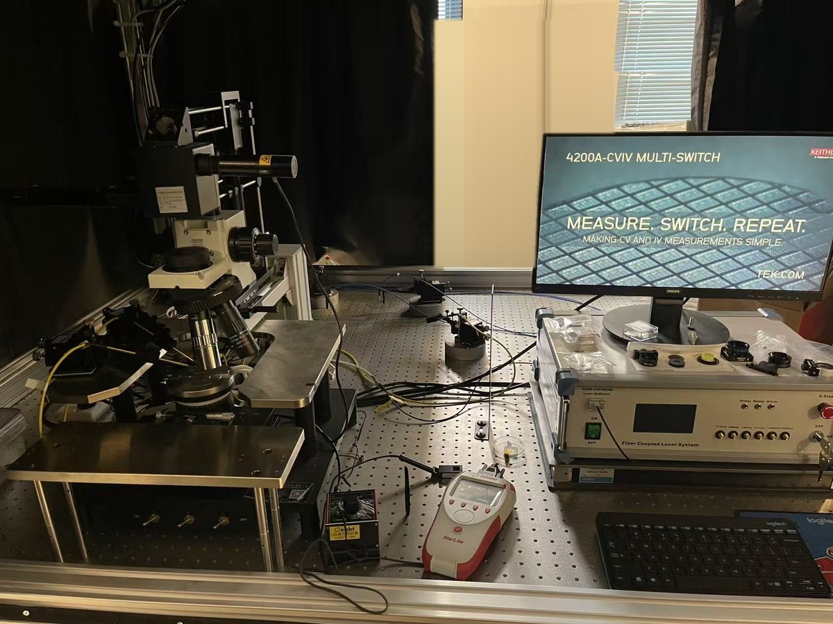
Photodetection System
Type: In-house photodetection platform combining a microscope optical path, a probe station and a semiconductor parameter analyser
Location: Cleanroom, Building M
Technical Specifications:
- Excitation: 375–1550 nm multi-wavelength laser, 365–1050 nm LED, 254 / 365 nm UV sources
- Focusing and collection: 5× / 20× / 50× objectives giving micrometre-scale spots; shutter-controlled exposure
- Electrical measurement: Keithley 4200A-SCS semiconductor parameter analyser (DC 10 aA–1 A, C-V 1 kHz–10 MHz) plus two 2450 source meters
- Sample stage: CS-4 probe station for chips and wafers
Working principle:
The excitation beam is focused onto a micrometre-scale region of the sample and the device electrodes are connected to the parameter analyser through the probes. Switching between illuminated and dark states yields photocurrent, dark current, I-V, C-V and pulsed response; changing wavelength and polarisation gives the spectral and polarisation dependence of the photoresponse.
Main Functions:
- Micro-area photoresponse of individual devices or structures
- Multi-wavelength and polarisation-resolved excitation from UV to near-infrared, with a polariser and half-wave plate
- Electrical characterisation: I-V, C-V and ultrafast pulsed I-V with 10 aA current resolution, suited to nanodevices with very low dark current
- Photocurrent mapping: point-by-point scanning gives the spatial distribution of the photocurrent
- Applications: responsivity, response time, dark current and noise of photodetectors; 2D materials, nanowires and metasurface devices